Glass Processing
Please feel free to consult with us on anything related to glass processing. We are capable of working with a
variety of materials, including single crystal materials.
We stock a wide range of products from Corning, SCHOTT, and Eagle to meet the diverse needs of our
customers.
We have extensive experience with custom orders for lenses, mirrors, and prisms.
Even in cases where other companies may quote a high price, please do not hesitate to contact us.
Laser System for Thick Glass Processing
The combination of a high-pulse-energy picosecond laser and our proprietary laser via-cutter with an extended focal depth enables precise cutting and drilling of thick glass (t ≧ 25 mm) and transparent materials.
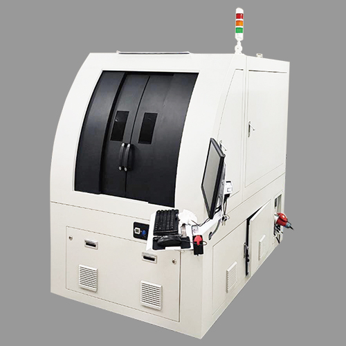
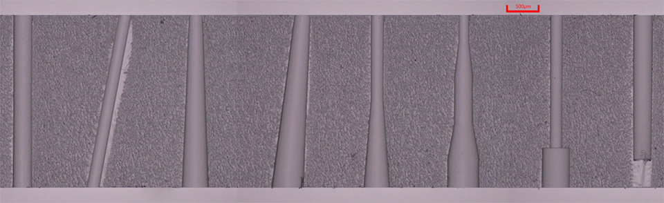
Reference Photos
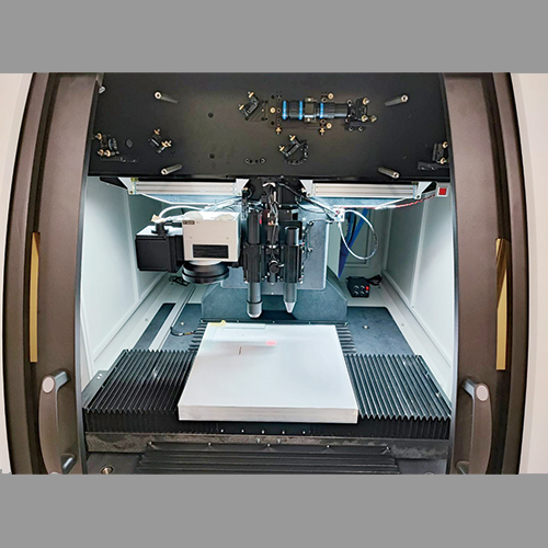
Reference Photos
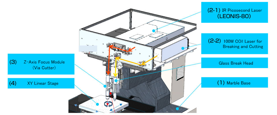
Layout Diagram of the Laser System for Thick Glass Processing
The via cutter head and glass break head are aligned in a single row from left to right corresponding to the laser beam path. The optical path adjustment frame is spatially offset and mounted on a vertical plate, and the entire assembly is finally protected by a dustproof cover.
(1) Marble Base: When designing the system as a precision processing machine, materials with high mass and low thermal expansion coefficients, such as marble, are used to minimize thermal expansion and inertial vibration.
(2-1) IR Picosecond Laser: Equipped with the LEONIS-80W for thick glass cutting.
(2-2) 100W CO2 Laser for Breaking and Cutting: Integrated 100W CO2 laser suitable for sheet glass cutting applications.
(3) Z-Axis Focus Module (Via Cutter): The optical system that narrows the irradiation beam according to the laser output specifications determines key parameters such as processing depth and aspect ratio.
(4) XY Linear Stage: The recommended stage size and precision vary depending on the workpiece and processing requirements.
Configuration of the Laser System for Thick Glass Processing
- Maximum worktable size: 400 x 400 mm
- Supported glass thickness: up to 30 mm
- Positioning accuracy: ±1.5 μm
- Equipped with SUPER WAVE LEONIS-80 (80 W @ 20 kHz, ≧ 4 mJ)
- Adopts a high-precision two-dimensional linear motor platform and a fully closed-loop control system to ensure accurate positioning and repeatability of the machine tool
- Equipped with a high-resolution CCD camera capable of automatic image recognition, high-precision visual positioning, and recognition of all types of silk-screen marks (target marks: round cross, diamond cross, and solid circle). The system can also recognize workpiece edges, chamfers, and drilled holes
- Incorporates an industrial-grade control computer for full software-based automation of all processing operations, providing excellent operability, machine stability, and reliable long-term continuous operation
- The high-rigidity structural design combines vibration-damping machine foot cups with a natural granite base to eliminate inertial vibration caused by table acceleration/deceleration and to prevent thermal deformation of the stage and related components
Specification Parameters
| Equipment |
Optional Laser |
Infrared Picosecond Laser
LEONIS-80 |
CO2 Laser |
| Laser Source (Wavelength / Type) |
Nano-, Pico-, and Femtosecond
1064, 532, 355 nm |
1064 nm Picosecond |
10.6 μm CO2 |
| Maximum Average Laser Power |
12–1500 W |
80 W @ 20 kHz, ≧ 4 mJ |
100 W |
| Type of Laser Processing |
Galvano Scanner + fθ Lens |
Via Cutter Head |
Focusing Lens |
| Laser Control Software |
Galvano Scanner
Control Software |
All-in-one Software for Cutting and Cracking
(Compatible with dxf, lcm, plt, txt, csv file formats) |
| Z-Axis Lift Module |
Z1 Axis, 100 mm Stroke |
| CCD Vision Positioning System |
Automatic Field-of-View Position Correction and Size Compensation
Field of View: 2.8 × 2.1 mm |
| X / Y Linear Motor Motion Stage |
Stroke: 500 × 500 mm, Speed: 500 mm/s, Acceleration: 0.8 G |
Positioning Accuracy
of X and Y Platforms |
±1.5 μm |
Repeatability Accuracy
of X and Y Platforms |
±1 μm |
| Total Weight |
1.6 t |
Required Facilities for Equipment Installation<
| Item |
Specification / Capacity |
| Power Supply |
Three-phase 200 V, 50–60 Hz |
| Compressed Air |
Pressure: > 0.5 MPa, Airflow: 200 L/min
Pipe Diameter: φ12 mm
*Please check in advance, as motor output varies depending on the power supply frequency. |
| Vacuum Source |
Vacuum generator integrated within the machine |
| Floor Load Capacity |
800 kg/m2 (per square meter) |
| Installation Ambient Temperature |
22 ± 3°C |
| Installation Environment Conditions |
Humidity: RH 62 ± 7% (no visible condensation allowed)
No rapid temperature changes, condensation, dust, or flammable materials. |
| Cleanliness Level |
Class 10,000 |
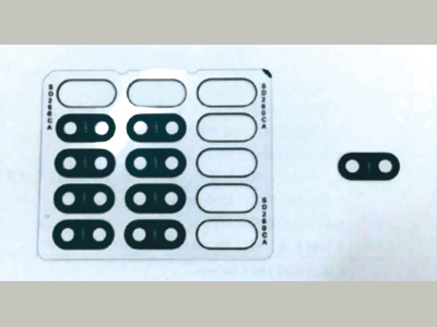
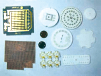
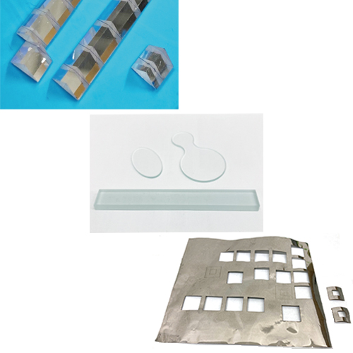
Processing Samples
Laser Cold Ablation Technology
Cold Ablation processing is a technology that enables precise microfabrication without leaving thermal
effects on the material.
This technique utilizes pulsed laser irradiation with ultra-short pulses, such as femtosecond lasers or
picosecond lasers.
In general, irradiation with ultra-short pulses shorter than 10 picoseconds generates minimal thermal
effects on the target material.
This makes it possible to microfabricate hard-to-process materials and high-hardness brittle
materials.
Its high peak energy induces nonlinear effects, which are used for cutting transparent materials and
micro-drilling.
Additionally, unique effects that do not appear in other laser thermal processes, such as generating
periodic structures on almost any material surface, have been observed, and the range of applications
continues to expand.
Glass
Cutting and Marking
Ceramic Processing
Drilling High-Hardness Brittle Materials
<Key Features>
High Peak Power:
The short pulse width generates high peak power, concentrating energy instantaneously at the focal
point.
Minimized Thermal Effects:
The extremely short pulse width completes processing before heat transfers to the material, reducing burrs,
cracks, and thermal deformation.
High-Precision Microfabrication:
Enables processing of fine structures and complex shapes, making it suitable for precision applications such
as electronic components and medical devices.
<Main Applications>
● Cutting: Dicing and micro-drilling of thin metal films, glass, sapphire, ceramics, and silicon
substrates
● Marking: Hydrophobic surface creation, QR code engraving, periodic surface structure formation, friction
reduction
● Modification: Optical waveguide formation, microchannel creation, micro-welding of transparent
materials
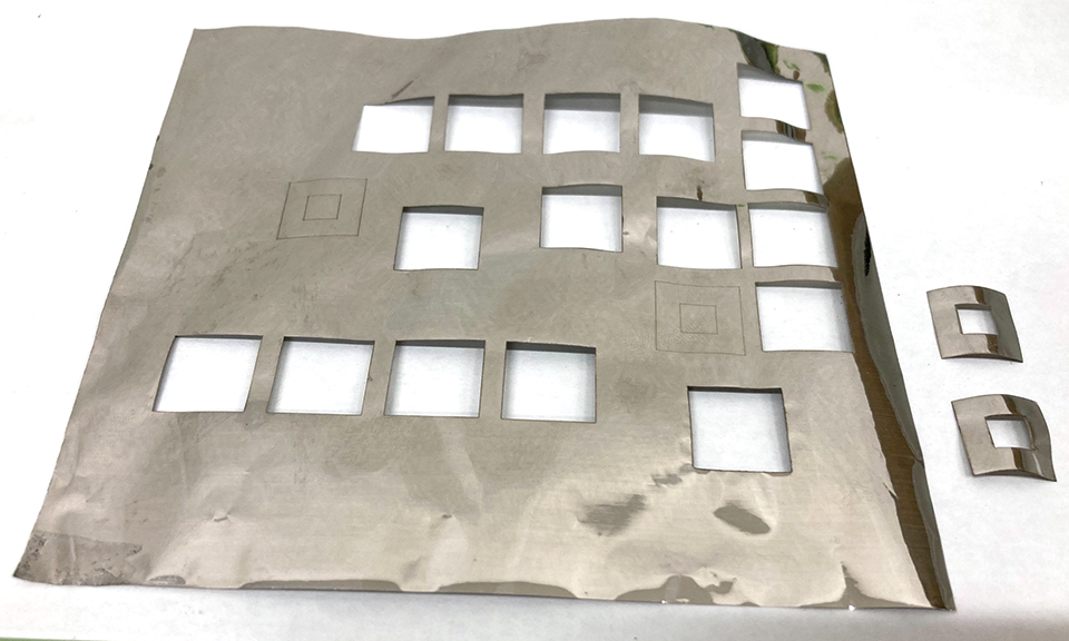
3D Glass Microfabrication
Shibuya Optical offers a wide range of three-dimensional glass microfabrication services.
We can process various geometries such as rings, squares, rectangles, regular cones, inverted cones, blind holes, angled holes, stepped holes, and other irregular shapes.
Please feel free to contact us for more information or custom designs.
Features
- Minimum aperture diameter: 30 μm
- Maximum aspect ratio: 1:100
- Glass thickness: 30 μm – 10 mm
- Glass size: 200 mm x 200 mm
- Materials: Synthetic quartz, TEMPAX, white glass, blue glass, etc.
- Surface: Free from microcracks or chipping; sidewall roughness less than 1 μm, providing a smooth finish
- Customization: Multiple angles, tapers, and structural geometries can be customized
Product Example
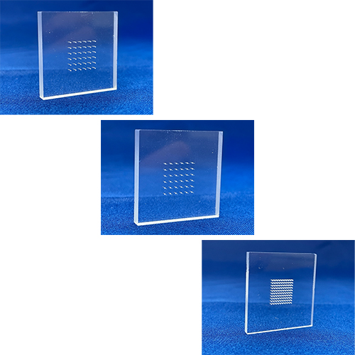
Optical Fiber Alignment Array
The optical fiber alignment array is a key component in optical communication systems, contributing to low-loss, high-speed, and large-capacity data transmission.
This product supports both one-dimensional and two-dimensional configurations, featuring high machining precision and excellent positioning accuracy.
- Tolerance: Precise positional and dimensional tolerance (±0.5 μm)
- Shape: Various shapes available, including straight holes, regular cones, and inverted cones
- Aperture Diameter: Available in 80 μm, 125 μm, 250 μm, and other sizes to meet diverse application needs
- Density: Typically high-density with 250 μm pitch spacing
- Angle: Vertical or inclined holes (e.g., 8° tilt)
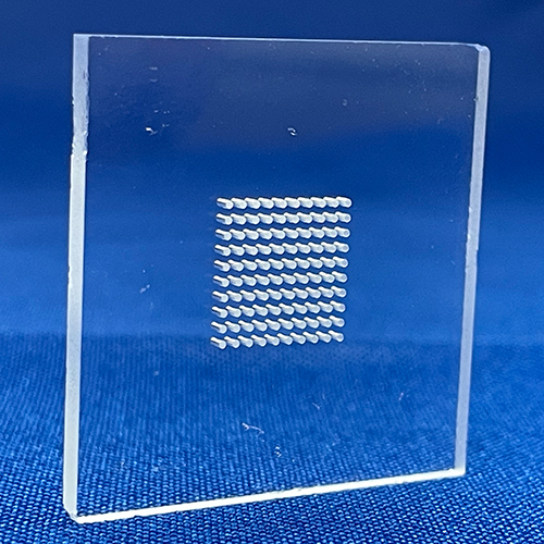
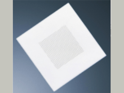
Reference Photo 1
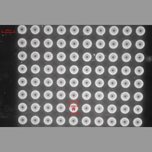
Reference Photo 2
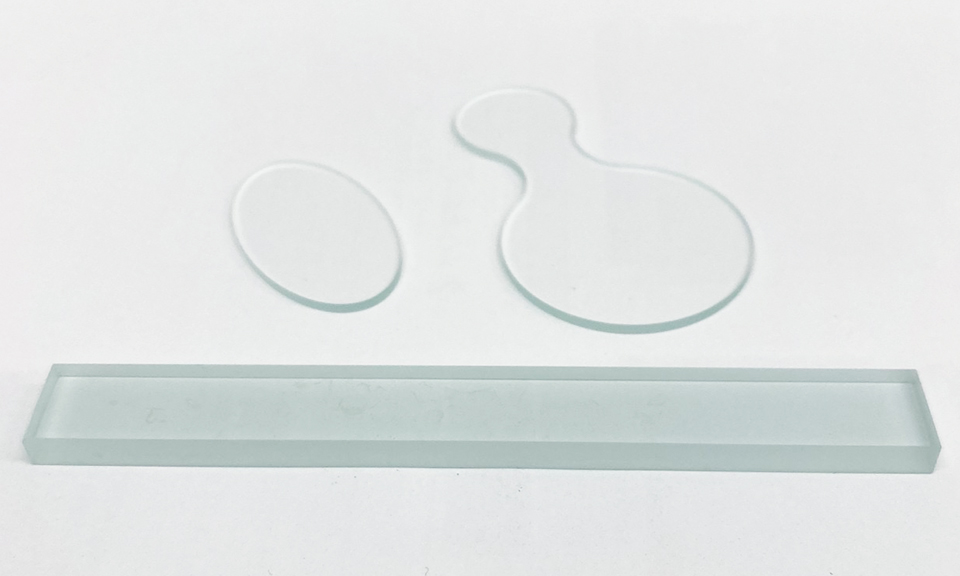
Microfluidic Glass Devices
Compared with conventional materials, quartz microstructures are well suited for a wide range of microfluidic technologies.
Based on various glass materials, we provide customized chips for multiple microfluidic applications.
These devices serve as key components in many fields, including cell analysis, cell biology, point-of-care diagnostics, and chemical synthesis.
- Minimum structural size: 1 μm
- Surface roughness: less than 1 μm (further reduced after polishing)
- Channel aspect ratio (width-to-depth): up to 1:100
- Substrate thickness: 100 μm – 10 mm
- Cutting: High-precision vertical or irregular cutting
- Surface: Free of residue, allowing easy bonding
- Cost and time: No molds required, enabling lower costs and shorter production times
- Customization: Fully customizable to match the customer’s unique design requirements
- Rapid prototyping: Quick prototype fabrication within 2–4 weeks, supporting high precision and multilayer designs
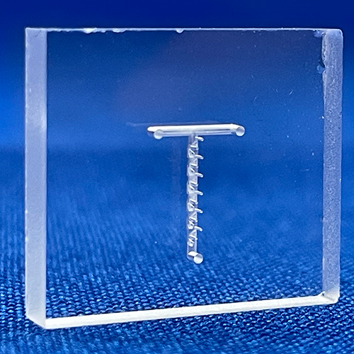
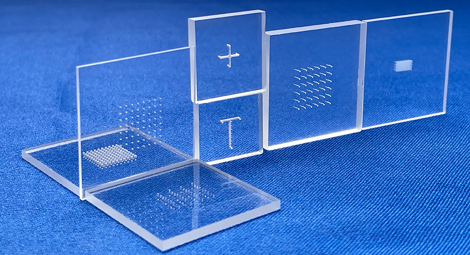
Reference Photo 1
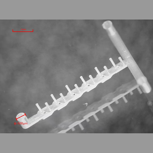
Reference Photo 2
Other Glass Processing Services
At Shibuya Optical, we offer processing services for a wide variety of glass materials.
By collaborating with our trusted partners both in Japan and overseas, we provide solutions tailored to each customer’s specific requirements.
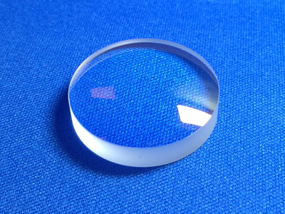
Lens
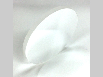
Mirror
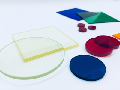
Color Glass
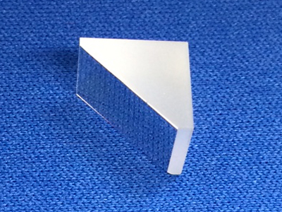
Prism
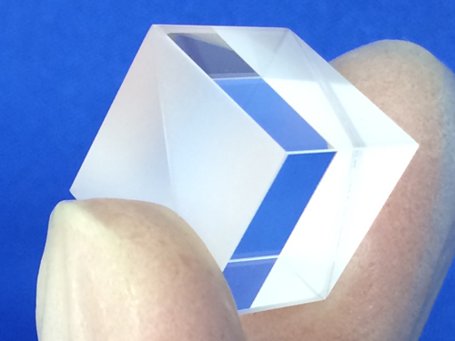
Beam splitter
ND Filter
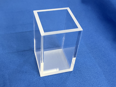
Glass Cell / Fused Silica Cell
<About Materials>
● Sapphire Glass ● Color Glass ● Fused Silica ● Chemically Strengthened Glass ● Blue Plate Glass ● White
Plate Glass
● Optical Glass (Equivalent to BK7) ● Heat-Resistant Glass (Tempax, Pyrex) ● Low-Expansion Glass
(Clearceram, Zerodur)
● Zero Expansion Crystallized Glass (Neoceram) ● Photomask Materials (Evaporated Substrates, Plated
Substrates) and more.
<About Processing Capabilities>
● Glass Polishing ● Cutting & Scribing ● Drilling ● Dicing & Machining
● Etching ● Coating & Deposition ● Machining and more.


 Processing Samples(
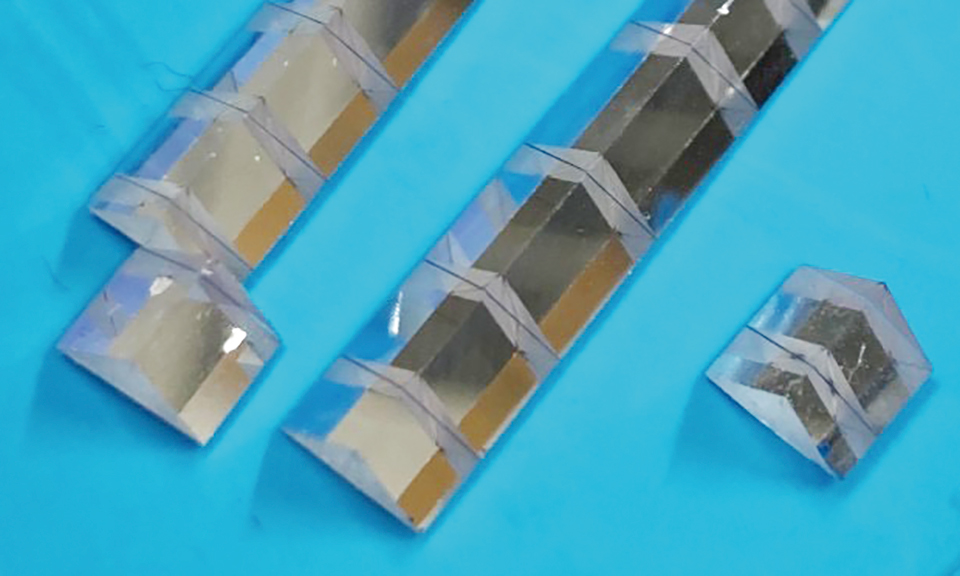
 Reference Photo 3(
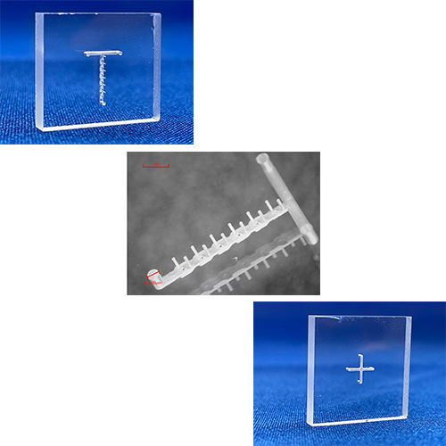 Reference Photo 3(